Solinsky Engineering Leadership Challenge: Manufacturing Success

Challenge On!
How Clarkson is Producing Career-Ready Engineers for Advanced Manufacturing
Ken ’71 and Grace Solinsky have made the single largest targeted financial commitment in Clarkson’s history. The Solinsky Engineering Leadership Challenge issues a bold call-to-action for the entire Clarkson community to engage in advancing the trajectory of engineering education, manufacturing research and technology, and our students' lives. The Solinskys’ historic $32M investment will match other donor commitments dollar-for-dollar in eight targeted areas, equipping Clarkson to deliver the highest impact engineering education in the country.
For more than 125 years, Clarkson has been producing highly successful graduates with the knowledge, hands-on experience and work ethic to be outstanding engineers and leaders. That is why more than 200 companies recruit students at our Spring and Fall Career Fairs and why our placement rates, starting salaries and lifetime career earnings are among the best in the nation.
Now, with the help of the Solinsky Engineering Leadership Challenge, we are positioned to lead the nation in preparing engineering graduates to become STEM leaders who solve global challenges and elevate advanced manufacturing.
Ken Solinsky graduated from Clarkson in 1971 with a BS in Mechanical Engineering. Grace Solinsky attended SUNY Potsdam from 1969-71 before transferring to East Texas State University, where she received her BS in Elementary Education. Ken began his career with the U.S. Army, where he progressed through a series of increasingly responsible engineering and management positions. In 1986, Ken left government service, and in 1997, he and Grace formed Insight Technology. Insight Technology grew from a startup to become the United States’ principal producer of Night Vision and Electro-Optical Systems, with over 1,300 employees. These systems are used by all branches of the U.S. Armed Forces, federal law enforcement agencies and allied nations. In 2010, Ken and Grace sold Insight Technology to L3 Communications. Ken then became President of L3 Warrior Systems, which encompassed Insight Technology as well as five other divisions with over 2,100 employees producing image intensifier tubes, infrared focal plane arrays, advanced laser systems, police dash cameras and holographic sights.

Other companies that the Solinskys started and still own include Rochester Precision Optics (RPO), OnPoint Systems and Envision Technology. RPO was formed in 2005 with the acquisition of the precision optics capabilities of Eastman Kodak. RPO produces precision optics and optical assemblies for defense, medical and consumer applications.
In 2015, Ken and Grace started OnPoint Systems. Its flagship product, SpotOn Virtual Smart Fence, a GPS-based dog collar, was named a CES 2020 Innovation Awards Honoree in the wearables category, named Product of the Year by the New Hampshire High Tech Alliance, named the Best Virtual Fence by WIRED magazine and given a People’s Choice Stevie Award for Favorite New Products at the 18th annual American Business Awards. In 2019, Ken founded Envision Technology. Envision develops advanced Night Vision and Electro-Optical Systems for the U.S. Military.
As the holders of 20 patents, recipients of numerous public sector and government awards, and owners of New York-based RPO, the Solinskys are not only established leaders in New York State industry but also are well known around the globe for their successes in manufacturing and engineering technology-driven business ventures. Ken and Grace Solinsky have been married for more than 50 years and are proud parents and grandparents.
Graduating Future STEM Leaders
Today’s economy demands engineers who can conceive, design, manufacture and rapidly bring to market products that address the toughest global challenges and most exciting business opportunities. To compete and lead in the global marketplace, our graduates must be prepared with not only the fundamental skills and hands-on experience necessary to start their careers, but also the ability to see the big picture and synthesize complex technical, manufacturing and business issues.
Through the Solinsky Engineering Leadership Challenge, we are reinvigorating the Clarkson experience to ensure that all our graduates gain valuable exposure to career opportunities in advanced manufacturing.
Building upon our existing SPEED programs, which provide essential hands-on experience, the Solinsky Challenge will ensure our students are equipped with critical understanding of innovative manufacturing practices and industry trends. By enhancing courses, labs, capstone projects, and integrating experiential learning across popular minors, microcredentialing and deeper industry partnerships, we are striving to deliver the highest-impact engineering education in the country.
Hands-on Learning Experiences Prepare Clarkson Graduates to be Career-Ready from Day One.

Enhanced Engineering Curriculum
Formal instruction on fundamental engineering and technical skills are enhanced through personalized advising and complemented by hands-on learning, interdisciplinary research, global and immersive experiences, internships and co-ops, SPEED Teams and more.

Personalized Complementary Learning
To better meet the needs of industry, we are introducing specialized, accelerated degree programs and providing our students with industry-relevant knowledge and skills through microcredential courses developed with employer partners and taught by experienced faculty.

Manufacturing Experiences and Leadership
Working in collaboration with industry, students gain practical manufacturing knowledge and valuable business perspectives through specialized seminars, internships and co-ops, research projects, plant tours and workforce development programs.
World-Class Faculty
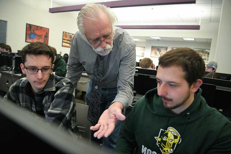
Our nationally recognized faculty have made Clarkson a top-tier research university. From receiving multimillion-dollar government grants to signing contracts with prominent industry partners, our faculty are experts in what they do both in the lab and in the classroom.

State-of-the-Art Facilities
The Solinsky Engineering Leadership Challenge will provide transformational enhancement and expansion of our classrooms, state-of-the-art research centers and labs, and specialized resources for innovation, entrepreneurship and early STEM education.
Technology Research and Transfer
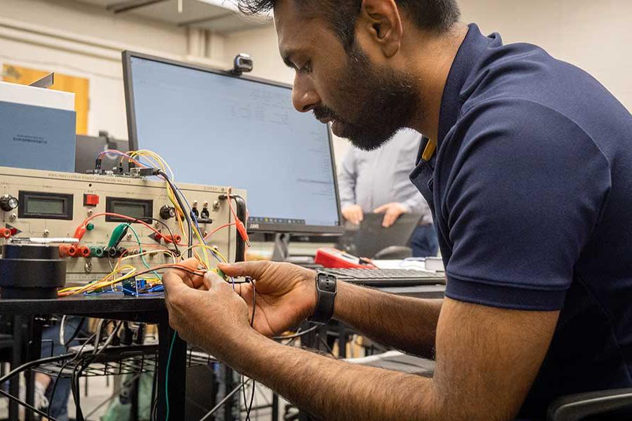
Clarkson is elevating its position as a thought leader and increasing its impact on Advanced Manufacturing innovation through focused research in critical sectors and enhanced collaboration with national labs, government entities and industry partners.
Together, We Rise to the Solinsky Engineering Leadership Challenge.
Industry Partners, Alumni and Friends of Clarkson can join us in creating the highest-impact engineering education in the nation through the eight areas of the Solinsky Engineering Leadership Challenge:
- Enhancing the Engineering Curriculum and Addressing 21st Century Advanced Manufacturing
- Personalized Complementary Learning by Fostering Industry and Alumni Interactions
- Attracting the Right People to Deliver on the Program Promise
- Advancing Manufacturing Leadership, Workforce Development and Thought Leadership
- Supporting Manufacturing and Industry Experience Programs for Students
- Increasing Tech Transfer & Research for Industry 4.0
- Learning and Doing in State-of-the-Art Facilities
- Meeting Industry Needs through a specialized 4+1 Master’s Program
Get involved today by contacting Development and Alumni Relations: (315) 268-7717 or email Steven Smalling, Associate Vice President for Development, steven.smalling@hwfj-art.com.
Student Success Stories
The Solinsky Engineers Program
If you are a high school student or someone who knows a high school student who wants to accelerate their personal and professional success in engineering and advanced manufacturing, this is a one-of-a-kind program to start day 1 learning and doing engineering.
Clarkson University's Wallace H. Coulter School of Engineering and Applied Sciences offers the Solinsky Engineers Program, bringing up to 100 of the University's top first-year engineering talent together to live, learn and grow each year.
Powering Manufacturing Innovation through Research
Discover how the Solinsky Engineering Leadership Challenge is powering technology transfer and research in key areas of innovation for the manufacturing industry.
Advanced Aerospace Material Development
PFAS Treatment and Remediation

Semiconductor Industry Technology
Advancing Aerospace Materials
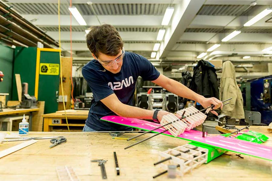
Advanced aerospace materials research is essential in today’s global marketplace, where the demand for stronger, lighter and more cost-effective materials is ever- increasing. Aerospace and defense industries, as well as manufacturers worldwide, rely on materials that not only perform under extreme conditions but also have extended lifespans and lower production costs. Traditional materials and mechanical fasteners, though reliable, add significant weight and present multiple points for potential failure in aerospace structures. Adhesive bonding offers a promising alternative, but achieving the same level of strength and consistency as traditional methods is a major obstacle – particularly in industries like aerospace and defense, where safety standards are stringent, and any unexpected material or joint failure could have severe consequences.
Clarkson University researchers are working to improve manufacturing processes through new predictive models and a better understanding of material failure from production through the end of life. At the Center for Advanced Materials Processing (CAMP), and with support from the Solinsky Engineering Leadership Challenge, Clarkson University researchers are helping aerospace manufacturers develop solutions that enhance material quality, reduce production costs and extend product life.
Our research is helping to solve the toughest challenges in aerospace and defense manufacturing and driving the next wave of technological innovation toward a more safe, efficient and sustainable future.
Featured projects:
Clarkson University’s Marcias Martinez and his research team are breaking new ground in aerospace materials with a project to make adhesive joints stronger and more reliable for U.S. Navy aircraft and vessels. Adhesive joints, which could replace metal fasteners, offer big advantages by reducing weight and cutting manufacturing costs. However, these joints aren’t yet widely used because it’s difficult to predict their strength and durability over time. To change that, the team is developing a model that accurately predicts how these adhesive bonds will hold up across their lifespan. Through a mix of material testing, advanced computer simulations and real-world validation, they’re creating a reliable framework to ensure adhesive joints meet the rigorous standards of the Navy and the aerospace industry. Backed by the Office of Naval Research and conducted in Clarkson’s new ATLAS Lab and HolSIP Lab, this work has the potential to revolutionize aerospace design by making adhesive bonds a practical and safe alternative to traditional metal fasteners.
PFAS Treatment and Remediation
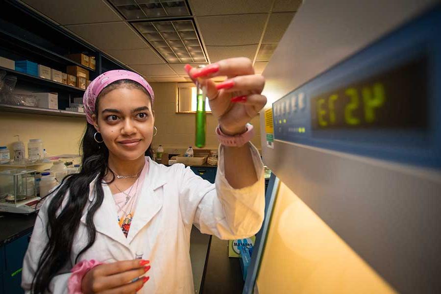
PFAS (Per- and PolyFluoroAlkyl Substances), often called “forever chemicals,” are synthetic compounds that have been used extensively in industrial and consumer products since the 1940s. PFAS are known for their durability and resistance to heat, water and stains; however, they have proven highly persistent in the environment and are now known to pose significant risks to human health and ecosystems. Once released from industrial sites, landfills or water runoff, PFAS accumulate in water, soil and living organisms – persisting indefinitely and contributing to toxic buildup over time. As regulatory restrictions increase, conventional methods of destroying PFAS remain costly and can produce harmful byproducts, so innovative solutions must be developed to safely and permanently eliminate these substances.
Clarkson University is at the forefront of developing effective PFAS remediation technologies. Through specialized research centers such as the Center for Air and Aquatic Resources Engineering and Sciences (CAARES), the Center for Advanced Materials Processing (CAMP) and the NYS Center of Excellence in Healthy Water Solutions, and with support from the Solinsky Engineering Leadership Challenge, our researchers are developing methods to safely and permanently eliminate PFAS from the environment.
We are pioneering sustainable PFAS remediation technologies and wastewater treatment solutions that will help protect public health while enabling industry to adopt cleaner practices and set new standards for environmental stewardship.
Featured projects:
Clarkson University’s Yang group, led by professor Yang Yang, is pioneering groundbreaking, non-thermal methods to safely destroy PFAS. Unlike traditional incineration of PFAS, the Yang group’s innovative room-temperature methods — like a photo-electrochemical system and piezoelectric ball milling — offer safer, energy-efficient alternatives. As published in Nature Water and Environmental Science & Technology Letters, their methods reflect Clarkson’s commitment to sustainable engineering and have drawn substantial support from the National Science Foundation as well as the U.S. Department of Energy and Department of Defense. Through partnerships with industry leaders such as TetraTech and CDM Smith, the team’s work is setting new standards in environmental management and positioning Clarkson at the forefront of sustainable, industry-aligned solutions for a cleaner future.
Read more about the Yang group’s innovative PFAS mitigation methods
Clarkson University professors Selma Mededovic Thagard and Thomas Holsen are tackling the issue of PFAS contamination in semiconductor manufacturing wastewater, a critical environmental challenge in the tech industry. PFAS are not only introduced as semiconductor manufacturing inputs but can also form during production, leading to persistent wastewater contamination. The Clarkson team’s research focuses on understanding where these contaminants come from and developing effective methods to eliminate them. Working with industry partners like GlobalFoundries and the Semiconductor Research Corporation, the researchers analyze wastewater samples to identify PFAS types and concentrations. Their findings are guiding the design of scalable treatment systems that aim to make semiconductor manufacturing more sustainable and environmentally responsible.
Read more about this research in Chemical & Engineering News
Semiconductor Industry Innovation
Technological innovation is critical to semiconductor manufacturing, where constant advancements are required to meet the growing demand for faster, smaller and more powerful electronic devices. From smartphones and computers to electric vehicles and renewable energy systems, semiconductors power the technologies shaping our modern world. As manufacturing techniques evolve, so do the challenges of maintaining efficiency, environmental responsibility and resource conservation. Addressing these issues requires advanced research to develop sustainable processes that reduce waste, limit harmful chemicals and improve energy efficiency in semiconductor production.
Clarkson University researchers are at the forefront of these efforts, conducting groundbreaking research aimed at creating safer, more eco-friendly practices for the industry. Through the Solinsky Engineering Leadership Challenge and our state-of-the-art labs and facilities at the Center for Advanced Materials Processing (CAMP) and Center for Air and Aquatic Resources Engineering and Sciences (CAARES), we are uniquely equipped to lead this charge.
Our innovative research on Chemical Mechanical Planarization and the remediation of pollutants in industrial wastewater is setting new standards for sustainable growth in semiconductor manufacturing, helping build a future where technological progress and environmental stewardship go hand in hand.
Featured projects:
Clarkson University’s Jihoon Seo and his team are examining the environmental impact of consumables used in Chemical Mechanical Planarization (CMP), a critical process in semiconductor manufacturing. With the rapid growth of the semiconductor industry driven by innovations in AI and IoT, the demand for CMP consumables — such as slurries, pads, brushes and cleaning solutions — has surged, leading to considerable environmental challenges. This research provides an in-depth life cycle assessment of these materials, highlighting their high energy and water use, hazardous material consumption and contribution to greenhouse gas emissions. By partnering with industry experts at Micron Technology, the Clarkson team is identifying key areas where sustainability improvements can be made. Their findings aim to guide the industry toward eco-friendly manufacturing practices, advocating for collaborative efforts among chipmakers, consumable producers and academic institutions to reduce the environmental footprint of CMP processes and advance sustainable manufacturing in the semiconductor industry.
Read about Clarkson’s CMP environmental impact research in ACS Sustainable Chemistry & Engineering
Clarkson University’s Jihoon Seo's research team is working to make semiconductor manufacturing safer for the environment by developing a new, eco-friendly polishing solution to replace the harmful chemicals currently applied during Chemical Mechanical Planarization (CMP) – an essential process in creating smooth copper and cobalt surfaces for electronics. The team is exploring natural amino acids, which are safer and help reduce harmful waste without sacrificing quality. With the support of major industry players like Intel and IBM, their research could lead to more efficient and sustainable practices in semiconductor manufacturing — a big step forward for the largest sector in the global manufacturing landscape.
Discover Clarkson’s natural slurry research in ScienceDirect
Clarkson University’s Jihoon Seo and his team are improving a key polishing process used in making semiconductors, the components found in almost every electronic device. This process, called Chemical Mechanical Planarization (CMP), smooths out surfaces like silicon dioxide to ensure they’re ready for building tiny, intricate electronic circuits. To make CMP more effective, the team is working with cerium dioxide particles, a type of fine abrasive, and studying how these particles interact with surfaces at the atomic level. Their research revealed that superfine particles made from certain materials polish more effectively and create fewer defects than conventional methods. Using specialized equipment at Clarkson’s Center for Advanced Materials Processing (CAMP), this research promises to make semiconductor manufacturing cleaner and more precise, helping the industry keep up with demands for smaller, faster and more reliable technology.
Explore Clarkson’s atomic-level insights for optimizing CMP on ScienceDirect
